- 您现在的位置:买卖IC网 > Sheet目录492 > NTP52N10G (ON Semiconductor)MOSFET N-CH 100V 60A TO220AB
�� �
�
�NTP52N10�
�Power� MOSFET�
�60� Amps,� 100� Volts�
�N� ?� Channel� Enhancement� Mode� TO� ?� 220�
�Features�
�?� Source� ?� to� ?� Drain� Diode� Recovery� Time� comparable� to� a� Discrete�
�Fast� Recovery� Diode�
�?� Avalanche� Energy� Specified�
�?� I� DSS� and� R� DS(on)� Specified� at� Elevated� Temperature�
�?� Pb� ?� Free� Package� is� Available*�
�Applications�
�?� PWM� Motor� Controls�
�?� Power� Supplies�
�?� Converters�
�MAXIMUM� RATINGS� (T� C� =� 25� °� C� unless� otherwise� noted)�
�http://onsemi.com�
�60� AMPERES�
�100� VOLTS�
�30� m� W� @� V� GS� =� 10� V�
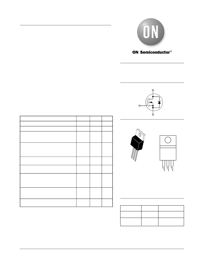
�N� ?� Channel�
�D�
�G�
�S�
�Rating�
�Symbol�
�Value�
�Unit�
�Drain� ?� to� ?� Source� Voltage�
�V� DSS�
�100�
�Vdc�
�MARKING� DIAGRAM� &�
�Drain� ?� to� ?� Source� Voltage� (R� GS� =� 1.0� M� W� )�
�Gate� ?� to� ?� Source� Voltage�
�?� Continuous�
�?� Non� ?� Repetitive� (t� p� v� 10� ms)�
�Drain�
�?� Continuous� @� T� A� 25� °� C�
�?� Continuous� @� T� A� 100� °� C�
�?� Pulsed� (Note� 1.)�
�Total� Power� Dissipation� @� T� A� 25� °� C�
�Derate� above� 25� °� C�
�Operating� and� Storage� Temperature� Range�
�Single� Drain� ?� to� ?� Source� Avalanche� Energy�
�?� Starting� T� J� =� 25� °� C�
�(V� DD� =� 50� V,� V� GS� =� 10� Vdc,�
�I� L� (pk)� =� 40� A,� L� =� 1.0� mH,� R� G� =� 25� W� )�
�Thermal� Resistance�
�?� Junction� ?� to� ?� Case�
�?� Junction� ?� to� ?� Ambient�
�V� DGR�
�V� GS�
�V� GSM�
�I� D�
�I� D�
�I� DM�
�P� D�
�T� J� ,� T� stg�
�E� AS�
�R� q� JC�
�R� q� JA�
�100�
�"� 20�
�"� 40�
�60�
�40�
�156�
�214�
�1.43�
�?� 55� to�
�+175�
�800�
�0.7�
�62.5�
�Vdc�
�Vdc�
�Adc�
�Watts�
�W/� °� C�
�°� C�
�mJ�
�°� C/W�
�4�
�1�
�2�
�3�
�TO� ?� 220�
�CASE� 221A�
�STYLE� 5�
�A�
�Y�
�WW�
�G�
�PIN� ASSIGNMENT�
�D�
�NTP52N10G�
�AYWW�
�1�
�G� D� S�
�=� Assembly� Location�
�=� Year�
�=� Work� Week�
�=� Pb� ?� Free� Package�
�Maximum� Lead� Temperature� for� Soldering�
�Purposes,� 1/8� ″� from� case� for� 10� seconds�
�T� L�
�260�
�°� C�
�ORDERING� INFORMATION�
�Stresses� exceeding� Maximum� Ratings� may� damage� the� device.� Maximum�
�Ratings� are� stress� ratings� only.� Functional� operation� above� the� Recommended�
�Operating� Conditions� is� not� implied.� Extended� exposure� to� stresses� above� the�
�Recommended� Operating� Conditions� may� affect� device� reliability.�
�1.� Pulse� Test:� Pulse� Width� =� 10� m� s,� Duty� Cycle� =� 2%.�
�*For� additional� information� on� our� Pb� ?� Free� strategy� and� soldering� details,� please�
�download� the� ON� Semiconductor� Soldering� and� Mounting� Techniques�
�Reference� Manual,� SOLDERRM/D.�
�Device�
�NTP52N10�
�NTP52N10G�
�Package�
�TO� ?� 220�
�TO� ?� 220�
�(Pb� ?� Free)�
�Shipping�
�50� Units� /� Rail�
�50� Units� /� Rail�
�?� Semiconductor� Components� Industries,� LLC,� 2006�
�March,� 2006� ?� Rev.� 4�
�1�
�Publication� Order� Number:�
�NTP52N10/D�
�发布紧急采购,3分钟左右您将得到回复。
相关PDF资料
NTP5404NRG
MOSFET N-CH 40V 136A TO220AB
NTP5860NLG
MOSFET N-CH 60V 220A TO-220-3
NTP5863NG
MOSFET N-CH 60V 97A TO-220AB
NTP5864NG
MOSFET N-CH 60V 63A TO-220
NTP60N06LG
MOSFET N-CH 60V 60A TO220AB
NTP65N02RG
MOSFET N-CH 25V 7.6A TO220AB
NTP75N03-006
MOSFET N-CH 30V 75A TO220AB
NTP75N03L09G
MOSFET N-CH 30V 75A TO220AB
相关代理商/技术参数
NTP5404N
制造商:ONSEMI 制造商全称:ON Semiconductor 功能描述:Power MOSFET 40 V, 136 A, Single N−Channel, D2PAK & TO−220
NTP5404NRG
功能描述:MOSFET NFET TO220 40V 136A 3.5mOhm RoHS:否 制造商:STMicroelectronics 晶体管极性:N-Channel 汲极/源极击穿电压:650 V 闸/源击穿电压:25 V 漏极连续电流:130 A 电阻汲极/源极 RDS(导通):0.014 Ohms 配置:Single 最大工作温度: 安装风格:Through Hole 封装 / 箱体:Max247 封装:Tube
NTP5411NG
功能描述:MOSFET 75A, 60V, 10mOhms N-Channel RoHS:否 制造商:STMicroelectronics 晶体管极性:N-Channel 汲极/源极击穿电压:650 V 闸/源击穿电压:25 V 漏极连续电流:130 A 电阻汲极/源极 RDS(导通):0.014 Ohms 配置:Single 最大工作温度: 安装风格:Through Hole 封装 / 箱体:Max247 封装:Tube
NTP5412NG
功能描述:MOSFET 60A, 60V, 10mOhms N-Channel RoHS:否 制造商:STMicroelectronics 晶体管极性:N-Channel 汲极/源极击穿电压:650 V 闸/源击穿电压:25 V 漏极连续电流:130 A 电阻汲极/源极 RDS(导通):0.014 Ohms 配置:Single 最大工作温度: 安装风格:Through Hole 封装 / 箱体:Max247 封装:Tube
NTP5426N
制造商:ONSEMI 制造商全称:ON Semiconductor 功能描述:Power MOSFET 120 Amps, 60 Volts N-Channel D2PAK, TO-220
NTP5426NG
功能描述:MOSFET 60V, 4.5mOhms N-Channel RoHS:否 制造商:STMicroelectronics 晶体管极性:N-Channel 汲极/源极击穿电压:650 V 闸/源击穿电压:25 V 漏极连续电流:130 A 电阻汲极/源极 RDS(导通):0.014 Ohms 配置:Single 最大工作温度: 安装风格:Through Hole 封装 / 箱体:Max247 封装:Tube
NTP5860N
制造商:ONSEMI 制造商全称:ON Semiconductor 功能描述:N-Channel Power MOSFET
NTP5860NG
功能描述:MOSFET
RoHS:否 制造商:STMicroelectronics 晶体管极性:N-Channel 汲极/源极击穿电压:650 V 闸/源击穿电压:25 V 漏极连续电流:130 A 电阻汲极/源极 RDS(导通):0.014 Ohms 配置:Single 最大工作温度: 安装风格:Through Hole 封装 / 箱体:Max247 封装:Tube